Product Summary
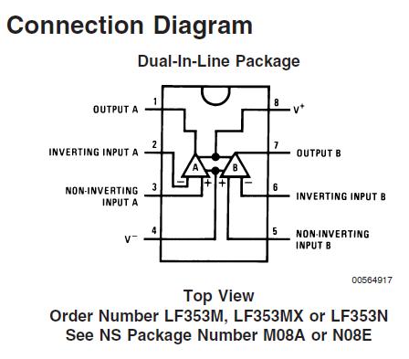
The LF353MX device is a low cost, high speed, dual JFET input operational amplifier with an internally trimmed input offset voltage (BI-FET II technology). It requires low supply current yet maintain a large gain bandwidth product and fast slew rate. In addition, well matched high voltage JFET input devices provide very low input bias and offset currents
Parametrics
Absolute maximum ratings: (1)Supply Voltage: ±18V; (2)Operating Temperature Range: 0℃ to +70℃; (3)Tj(MAX): 150℃; (4)Differential Input Voltage: ±30V; (5)Input Voltage Range: ±15V; (6)Output Short Circuit Duration: Continuous; (7)Storage Temperature Range: -65℃ to +150℃; (8)Lead Temp. (Soldering, 10 sec.): 260℃; (9)Soldering Information Dual-In-Line Package Soldering (10 sec.): 260℃.
Features
Features: (1)Internally trimmed offset voltage: 10 mV; (2)Low input bias current: 50pA; (3)Low input noise voltage: 25 nV/√Hz; (4)Low input noise current: 0.01 pA/√Hz; (5)Wide gain bandwidth: 4 MHz; (6)High slew rate: 13 V/μs; (7)Low supply current: 3.6 mA; (8)High input impedance: 1012Ω; (9)Low total harmonic distortion : ≤0.02%; (10)Low 1/f noise corner: 50 Hz; (11)Fast settling time to 0.01%: 2 μs.
Diagrams

| Image | Part No | Mfg | Description |  |
Pricing (USD) |
Quantity | ||||||||||||
|---|---|---|---|---|---|---|---|---|---|---|---|---|---|---|---|---|---|---|
 |
 LF353MX |
 Fairchild Semiconductor |
 Operational Amplifiers - Op Amps Dual Op amp JFET |
 Data Sheet |

|
|
||||||||||||
 |
 LF353MX/NOPB |
 National Semiconductor (TI) |
 Operational Amplifiers - Op Amps WIDE BW DUAL JFET INPUT OP AMP |
 Data Sheet |

|
|
||||||||||||
 (China (Mainland))


